
Introduction
We choose wrong sensors, test them under unrealistic conditions, and uncover critical issues only when nearing EVT (Engineering Validation Test) or DVT (Design Validation Test). At that point, the wrong sensor doesn’t just affect the performance – it creates redesign loops, derails timelines, and inflates costs. For hardware founders and OEM (Original Equipment Manufacturer) decision makers operating in an increasingly accelerated market, understanding how imaging decisions unfold in the real world is essential. The right choice empowers reliability and scalability; the wrong one can compromise the entire product’s roadmap.
CMOS vs. CCD: The First Strategic Choice
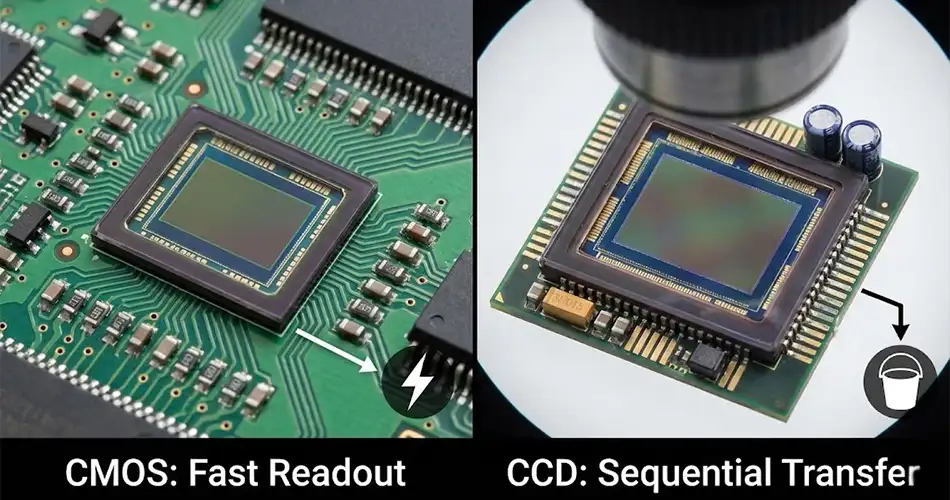
CMOS has become the dominant choice for modern hardware because it aligns with fast-paced, cost-conscious product development. Imagine a service robot navigating a supermarket. It needs rapid readout speeds, low power consumption, and the ability to run on-device AI without overwhelming the processor. CMOS sensors thrive here: they integrate amplification and conversion directly on-chip, enabling efficient real-time imaging without heavy surrounding electronics. Their affordability also matters, especially when scaling tens of thousands of units. CCD shines in a different world entirely. Think of a microscopic imaging device in a laboratory or a satellite capturing Earth observation data. In these cases, uniformity and ultra-low noise matter more than power or cost. CCD provides exceptional accuracy, clean signals, and consistent pixel behavior across the frame. But these benefits come with trade-offs: higher power draw, slower readout, and larger supporting circuitry. In applications demanding scientific precision, CCD is irreplaceable. But for most commercial and industrial products, CMOS delivers the right balance of performance, efficiency, and scalability.
Feature-by-Feature Comparison
| Attribute | CMOS (Complementary Metal-Oxide-Semiconductor) | CCD (Charge-Coupled Device) |
|---|---|---|
| Readout Speed | Fast; ideal for real-time processing | Slow; sequential charge transfer |
| Power Consumption | Low; optimized for embedded systems | High due to charge pumping |
| Noise Performance | Variable; improved with modern designs | Extremely low; high uniformity |
| System Complexity | Lower; on-chip circuitry integrated | Higher; requires external components |
| Cost Structure | Cost-efficient for mass production | Higher fabrication and BOM cost |
| Best Use Cases | Robotics, consumer devices, embedded vision | Aerospace, microscopy, scientific imaging |
Low-Light Sensors: Engineering for Real-World Conditions

Consider a home security device that must clearly identify activity at 2 a.m. Traditional sensors deliver grainy, unreliable output under such conditions. Low-light sensors equipped with backside illumination, larger pixel wells, and enhanced NIR (Near-Infrared) sensitivity, capture significantly more detail. Similarly, medical devices used in subdued hospital rooms rely on low-light performance to ensure sensor accuracy without forcing harsh illumination. In autonomous mobile robots, poor low-light visibility can directly translate to safety risks; a missed object or incorrect depth estimation can derail operations. Low-light imaging ensures that your product doesn’t just work in ideal conditions; it works everywhere your customer expects it to.
Depth Cameras: Enabling Spatial Intelligence
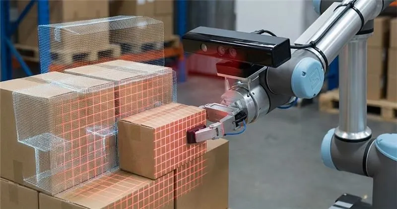
In a warehouse, an autonomous mobile robot depends on depth sensing to avoid forklifts, recognize pallet edges, and navigate tight aisles. Stereo depth systems offer cost-effective outdoor performance, structured-light shines in controlled indoor scanning environments, and Time-of-Flight (ToF) cameras deliver real-time, stable depth mapping even with fast motion and dynamic lighting.
Depth technology becomes even more vital in AR/VR devices, biometric verification, and gesture-control platforms. Without accurate depth perception, interactions become unreliable, and user trust rapidly erodes. The right depth camera ensures your product understands distance, shape, movement, and environment (qualities that directly impact safety), user experience, and operational efficiency.
Thermal Imaging: Seeing Outside the Visible Spectrum
Thermal imaging unlocks a spectrum of information invisible to the human eye, and when paired with AI, it can be transformative. In industrial settings, thermal modules identify overheating machinery long before a failure occurs. In emergency response, robots equipped with thermal vision can find trapped individuals through smoke or darkness.
But thermal sensors behave very differently from RGB (Red, Green, Blue) modules. They require calibration to account for drifts. They use specialized optics- often germanium, that influences cost and durability. Their resolution is typically lower, so software interpolation and thermal-AI pipelines become essential for meaningful output. Without understanding these nuances, teams often misjudge what thermal imaging can and cannot do.
Selecting the right thermal module ensures your product can interpret heat, identify anomalies, and operate in environments where visible-light sensors simply cannot function.
Imaging as a System-Level Decision
Treating imaging as a system-level decision ensures that sensor choice aligns with compute capability, thermal margins, power availability, mechanical layout, and long-term sourcing before you enter EVT (Engineering Validation Test). This alignment is the difference between smooth scaling and costly iteration.
A Practical Roadmap for Product Teams
To avoid late-stage surprises, teams should follow a structured imaging roadmap:
- Identify the primary imaging mission – clarity, low-light reliability, depth perception, thermal sensing, or cost optimization.
- Map real-world deployment conditions – lighting, movement, reflectivity, temperature swings, and environmental hazards.
- Evaluate how each sensor family behaves in those conditions – not in a lab, but in the actual frontline environments.
- Early testing with prototypes – real use always reveals insights that spec sheets hide.
- Validate supply chain reliability – sensor longevity must match your product’s manufacturing roadmap.
Why Rapidise Becomes the Right Engineering Partner
Imaging may be complex, but with Rapidise, it becomes a strategic advantage rather than a technical hurdle. If you’re building a device that depends on vision or spatial intelligence, our engineering and manufacturing teams ensure you choose the right sensor and transform it into a fully integrated, production-ready imaging system.